
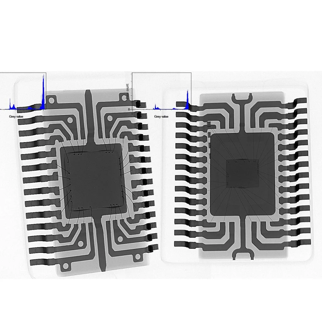
To start, we introduce a key pillar of our quality control : X-ray inspection .
With our X-ray inspection system , we ensure the quality of electronic assemblies, PCBs, and components . This technology enables the inspection of hidden or hard-to-access components that are not visible using traditional inspection methods like Automated Optical Inspection (AOI) .
1. Quality Control and Defect Detection
• Solder joint inspection: Analysis of solder connections, especially for BGA and QFN components, which are hidden beneath the package.
• Through-hole solder penetration: Verification of solder fill levels in THT component connections .
• Voids in solder joints: Detection of air pockets, cavities, or irregularities in soldering.
• Short circuits and interruptions in PCBs: Identification of shorts or breaks in inner PCB layers .
2. Process Optimization
• Manufacturing process analysis: Fine-tuning soldering processes and stencil printing to improve quality and reduce defect rates.
• Preventive measures: Early detection of potential weak points , such as problematic solder joints , before they cause larger failures.
3. Product Validation
• Prototype inspection: Supporting customers during development to ensure that new designs and prototypes meet quality standards.
• Mass production: First-article inspections and sample testing to maintain consistent product quality .
4. Failure Analysis
• Defect investigation: Identifying production errors or material defects to determine root causes and corrective actions.
• Detection of broken bond wires, structural damage, and counterfeit ICs , preventing issues caused by manipulated components .
5. Benefits of X-Ray Inspection
✅ Non-destructive testing: Components remain undamaged during inspection.
✅ High precision: Even the smallest defects are detectable.
✅ Time and cost savings: Helps prevent future failures and costly recalls .
Conclusion
X-ray inspection is an indispensable tool in modern electronics manufacturing . It ensures quality, reliability, and longevity —especially for complex and densely packed PCB designs .